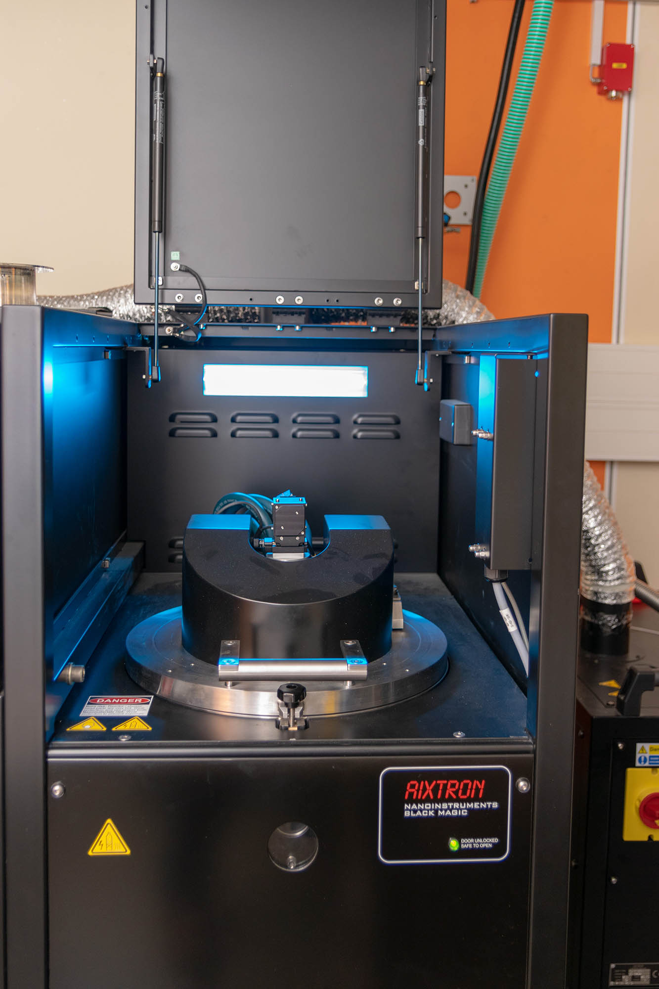
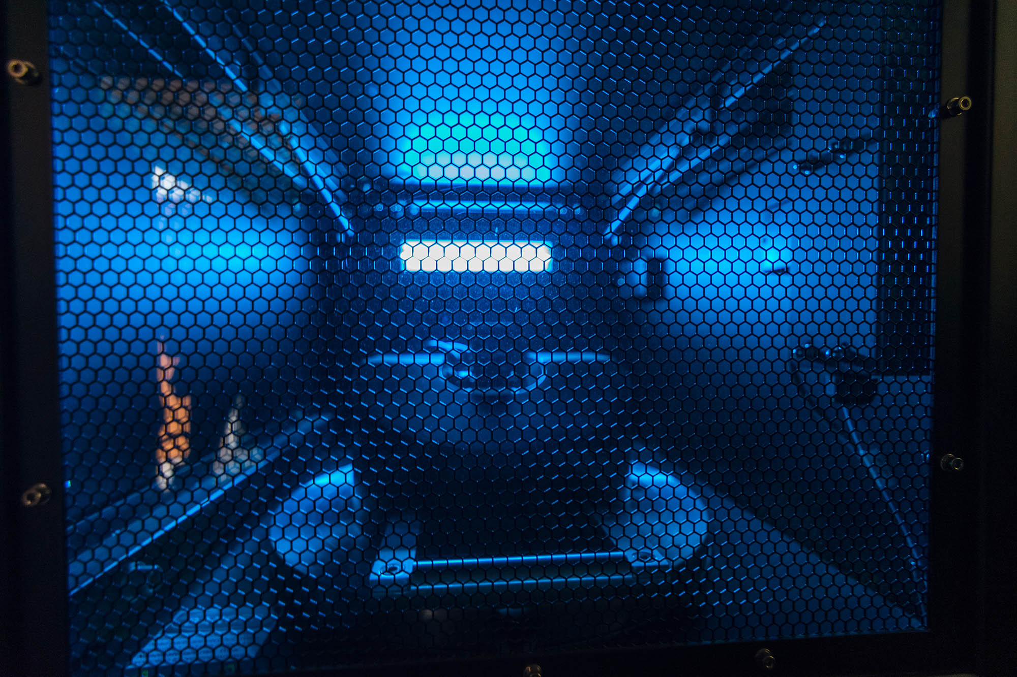
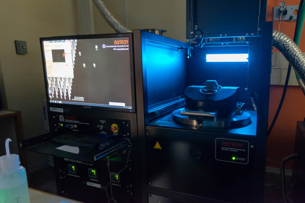
Chemical vapor deposition (CVD) is a technique used to produce thin films of materials. In CVD process, a substrate is heated to high temperature and exposed to precursor gases, which react or decompose on the substrate surface to form a coating of the required material. More specifically, CVD synthesis of materials consists of three steps: Firstly, an appropriate substrate is heated to the growth temperature, while certain gases are flowing to remove any impurities on substrate surface. Then precursor gases are introduced into the reaction chamber and by suitable conditions of pressure, temperature, etc., a coating of the desired material is formed on substrate. Growth continues until precursor gases flow is terminated and finally, on the last step, chamber is cooled down to room temperature.
CVD process can be successfully used for the production of high quality graphene. For this, metal substrates, methane gas as precursor material, low pressures and temperatures of ~ 1000 °C are used. Also, other process gases, such as argon and hydrogen, may be present. Common substrates include copper and nickel. Copper substrates are particularly attractive, since copper is an excellent catalyst for the graphene formation and also can be easily removed during graphene transfer to other substrates.

Initial goals aimed at the successful production of large scale, monolayer graphene. This is now achieved, amongst others, using copper foils as substrates. Understudying graphene growth mechanism and careful selection of gas flows, growth temperature, pressure and time can lead to the formation of large, monolayer graphene crystals.

Synthesis of high quality graphene is a key factor for the development of advanced technological applications like new generation optoelectronics, transistors, sensors, energy storage devises, composite materials etc.


